Designing your Own NFC Business Cards
Learn how to design and build your own NFC PCB business card using KiCad
An NFC PCB business card can be a fun and unique way to promote yourself or your business.
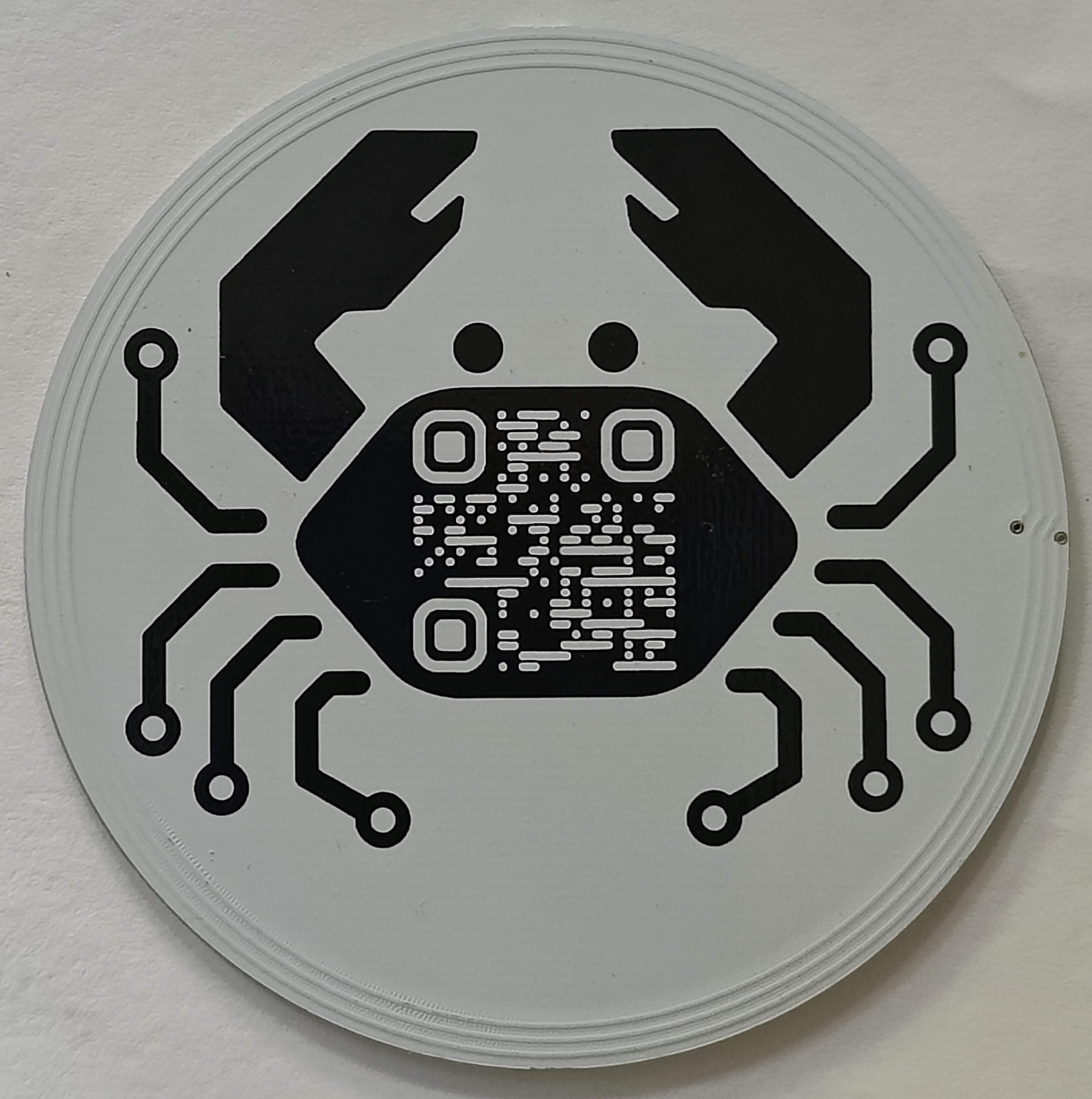
Crab Labs designed and built these NFC PCB Business cards, the source files are here

I will show you how to design and build one using KiCad and JLCPCB
Prerequisites
- Understanding of basic circuit theory and electronics (video here)
- Working knowledge of KiCad (Tutorial here)
Primer on NFC (Near Field Communication)
Near Field Communication is a standardized series of protocols which define communication between two devices utilizing a 13.56 MHz carrier frequency (reference).
NFC devices need to be within several centimeters to communicate with each other.
Common NFC protocols are ISO 14443 (Most Common) and ISO 15693 (Newer, faster, more range). Most devices, including smartphones, natively support ISO 14443 communication; support for ISO15693 is not as widespread.
There are two main classes of NFC devices, Tags and Readers. This business card will be a tag and a smartphone or other device will be a reader.
NFC Tags store information that is procedurally read by a reader device when it gets close enough to be powered by it. The format and type of data that is read and interpreted is standardized but may or may not be supported based on the reader.
Preliminary Design
The first step in the design is deciding the big picture details of the design such the general shape of the card and what it will contain.
NFC Tags can have a large amount of data stored on then, some reader devices have less compatibility than others in regards to acting on the data in the tag. For example, contact cards (vCards) can be stored on NFC Tags but Apple IPhones are not able to automatically import or read them in to your contacts while most Android devices have native support.
The most universal data form is a simple url, it is recommended to store either a URL or phone number. If you or your company has a website or landing page that would be ideal.
As for the size and shape of the card there are very few limitations, the main limitation is in regards to the antenna. There should be an unbroken area of at least 2cm x 2cm which is dedicated for the NFC antenna, the larger the antenna is, the greater the range. You can and should create an interesting outline using tools such as Adobe Illustrator, Inkscape, or other Vector Graphics or CAD tools. Crab Labs recommends having no dimension greater than 3.5 inches (90 mm) in the x or y direction (a standard business card is 3.5” x 2” (90 x 50mm))
Crab Labs designed our version as a circle in order to use them as coasters or decor as well as to stand out.
Creating the Schematic
The following circuit is what was designed and used by Crab Labs
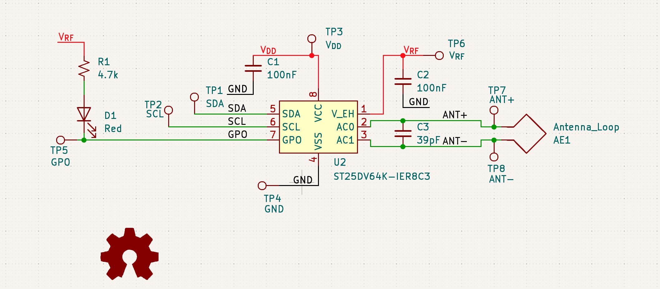
The circuit is relatively simple, it revolves around a NFC IC which handles all of the NFC communication.
More circuitry can be added as desired.
For a detailed breakdown of the schematic see the docs portion of the source repository located here.
Open KiCad and create a new project using Command+N or Ctrl+N
Find a location to create the project and name it something appropriate, such as “BusinessCard”
Once the project has been created, navigate to and open the schematic (the file called *.kicad_sch), it will look like this:
Selecting an NFC Tag IC
The most crucial decision in designing an NFC business card if the choice of NFC transponder or tag IC. It is generally recommended to chose a ISO 14443 chip as it is the most compatible.
There are a number of popular ISO 14443 NFC Tag ICs, such as:
Some of the most popular ISO 15693 NFC Tag ICs are:
- ST25DVx by ST Microelectronics (x = 04K, 16K, 64K)
- M24LRx by ST Microelectronics (x = 04, 16, 64)
- N24RFx by onsemi (x = 04, 16, 64)
The most important factor in finding the right transponder chip is the memory size, you generally want as much memory as you can afford.
Note: Crab Labs recommends using the M24S or ST25DV series of transponders, they are plentiful, affordable, and easy to work with.
Sourcing NFC Tag ICs
If you are comfortable hand soldering components you can look for components from any source (Octopart searches multiple sources around the web at once). Chose tags with SO-8 or similar packages if you plan to hand assemble unless you have access to advanced tools or have significant experience.
If you can’t or don’t want to hand assemble PCBAs, then it is recommended to look for components on LCSC. If the component is available on LCSC then your design can be fully built and assembled at JLCPCB in a timely manner. If you do not chose a component that is available on LCSC you will either have to hand assemble that component or have the part be ordered on the side (this is more expensive, takes longer, and is more difficult).
Open KiCad and create a new project using Command+N or Ctrl+N
Find a location to create the project and name it something appropriate, such as “BusinessCard”
Once the project has been created, navigate to and open the schematic (the file called *.kicad_sch), it will look like this:
Placing the Components
Once you have selected an NFC IC, you need to create symbols for it in KiCad. For information on how to import external components, see our guide on importing external libraries in KiCad.
Place the NFC IC symbol on your schematic and connect the antenna pins according to the datasheet specifications.
Antenna Design
The antenna is the most critical part of an NFC design. It needs to be properly tuned to 13.56 MHz for optimal performance. The antenna is typically a multi-turn coil that can be created directly on the PCB using copper traces.
Key considerations for antenna design:
- Number of turns (typically 3-7)
- Trace width and spacing
- Total inductance (usually 1-3 µH)
- Tuning capacitor value
Many NFC IC manufacturers provide antenna design calculators and reference designs that can be used as starting points.
PCB Layout
Once your schematic is complete, it’s time to move to the PCB layout. In KiCad:
- Update the PCB from the schematic
- Define your board outline (import your custom shape if you created one)
- Place components strategically
- Route the antenna coil
- Add any decorative elements or silkscreen artwork
Antenna Layout Tips
- Keep the antenna traces away from other components and ground planes
- Maintain consistent trace width and spacing
- Use smooth curves instead of sharp corners
- Consider using multiple PCB layers for complex designs
Manufacturing
For manufacturing, we recommend JLCPCB as they offer competitive prices for small batches of PCBs.
Preparing Files for JLCPCB
- Generate Gerber files from KiCad
- Create a drill file
- Generate pick-and-place files if using SMT assembly
- Create a BOM (Bill of Materials) if using assembly services
Ordering Process
- Upload your Gerber files to JLCPCB
- Select PCB specifications:
- 2 or 4 layer board
- 1.6mm thickness (standard business card thickness)
- HASL or ENIG surface finish
- Your choice of solder mask color
- If using assembly services, upload BOM and pick-and-place files
- Review and place your order
Programming the NFC Tag
Once you receive your manufactured PCB business cards, you’ll need to program the NFC tags with your data.
Tools for Programming
- NFC Tools (Mobile app for Android/iOS)
- TagWriter by NXP (Mobile app)
- Proxmark3 or similar NFC reader/writer for advanced users
Programming Steps
- Power on the NFC tag (if it has active components)
- Use your chosen tool to connect to the tag
- Write your data:
- URL to your website
- vCard with contact information
- Custom NDEF messages
- Lock the tag if desired (prevents overwriting)
Testing and Validation
After programming, test your NFC business cards with various devices:
- Different smartphone models (iPhone and Android)
- Various NFC reader applications
- Test read range and reliability
- Verify data integrity
Cost Analysis
Typical costs for a batch of 100 NFC PCB business cards:
- PCB manufacturing: $50-100
- NFC ICs: $0.50-2.00 per chip
- Assembly (if not hand-soldering): $50-100
- Total: ~$1-3 per card for 100 units
Troubleshooting Common Issues
Poor Read Range
- Check antenna tuning
- Verify proper impedance matching
- Ensure no metal objects are interfering
Inconsistent Reading
- Verify NFC IC is properly soldered
- Check for damaged antenna traces
- Test with multiple reader devices
Data Corruption
- Ensure proper NDEF formatting
- Verify memory isn’t corrupted
- Check power stability (for active tags)
Advanced Features
Consider adding these features to make your business card stand out:
- LED indicators that light up when read
- E-ink display for dynamic information
- Multiple NFC chips for different functions
- Environmental sensors with data logging
- Energy harvesting from the NFC field
Conclusion
Creating your own NFC PCB business card is an excellent way to showcase your technical skills while providing a memorable networking tool. With careful design and attention to detail, you can create a professional and functional business card that sets you apart from the crowd.
The entire process, from design to holding your finished cards, typically takes 2-3 weeks. The skills you learn in this project - PCB design, RF antenna design, and NFC programming - are valuable for many other embedded systems and IoT projects.
Remember to iterate on your design based on testing results, and don’t be afraid to experiment with different shapes, materials, and features to create something truly unique.
For the complete source files and additional documentation for our NFC business card design, visit our GitHub repository.